Avoiding common PCBA design mistakes ensures reliable prototypes and smooth production transitions. Engineers and OEMs can save time and costs by addressing these issues early in the design phase.
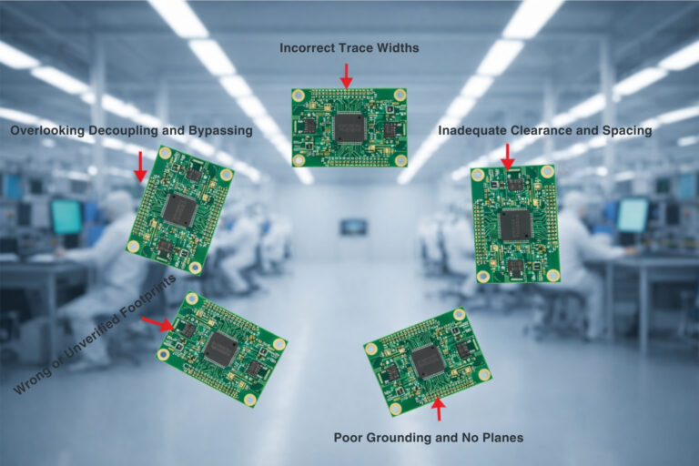
Mistake 1: Incorrect Trace Widths
Designers often use uniform trace widths across power, signals, and high-speed lines, leading to overheating or voltage drops. Always calculate widths based on current (e.g., 1A needs ~20 mil for 1oz copper) using IPC-2221 standards.
To avoid: Use online calculators or fab house tools; prioritize wider traces for power nets (50-100 mil) and verify with thermal simulations.
Mistake 2: Inadequate Clearance and Spacing
Placing traces or pads too close risks shorts during manufacturing or soldering, especially under IPC Class 2 rules (min 6 mil spacing).
To avoid: Run Design Rule Checks (DRC) in your EDA software; add 10-20% buffer for high-voltage areas and consult fab DFM guidelines.
Mistake 3: Poor Grounding and No Planes
Relying on trace routing for ground creates loops that amplify noise and EMI, failing compliance tests.
To avoid: Dedicate a full ground plane on inner layers for multi-layer boards; use vias to stitch planes and separate analog/digital grounds with a narrow bridge.
Mistake 4: Wrong or Unverified Footprints
Mismatched component footprints from libraries cause assembly failures, like pins not fitting pads.
To avoid: Cross-check datasheets for pad size, drill diameter, and polarity; create custom footprints and get a second review before Gerber export.
Mistake 5: Overlooking Decoupling and Bypassing
Skipping or misplacing decoupling capacitors near ICs leads to power supply noise and erratic behavior.
To avoid: Place 0.1µF caps within 5mm of every power pin, plus bulk caps (10-100µF); route short, wide paths to minimize inductance.
Quick Prevention Checklist
| Step | Action Item |
|---|
| Pre-Layout | Verify footprints and BOM |
| Routing | Size traces, check clearances |
| Review | Run DRC/DFM, simulate signals |
| Final | Export Gerbers, request fab review |
At Foshan Krivina PCBA, our free DFM analysis catches these pitfalls before production. Upload your design for expert feedback and fast-turn prototypes from China to India.
Get Started: Request your no-obligation design review today.